Youngmin Kim 1, Simone Assali 2, Hyo-Jun Joo 1, Sebastian Koelling 2, Melvina Chen 1, Lu Luo 2, Xuncheng Shi 1, Daniel Burt 1, Zoran Ikonic 3, Donguk Nam 1, Oussama Moutanabbir 2
1 School of Electrical and Electronic Engineering,Nanyang Technological University,50 Nanyang Avenue,Singapore 639798,Singapore.
2 Department of Engineering Physics, École Polytechnique de Montréal, C.P. 6079, Succ. Centre-Ville, Montréal, Quebec H3C 3A7, Canada.
3 School of Electronic and Electrical Engineering, University of Leeds, Leeds LS2 9JT, UK
Abstract:
Nanowires are promising platforms for realizing ultra-compact light sources for photonic integrated circuits. In contrast to impressive progress on light confinement and stimulated emission in III-V and II-VI semiconductor nanowires, there has been no experimental demonstration showing the potential to achieve strong cavity effects in a bottom-up grown single group-IV nanowire, which is a prerequisite for realizing silicon-compatible infrared nanolasers. Herein, we address this limitation and present an experimental observation of cavity-enhanced strong photoluminescence from a single Ge/GeSn core/shell nanowire. A sufficiently large Sn content ( ~10 at%) in the GeSn shell leads to a direct bandgap gain medium, allowing a strong reduction in material loss upon optical pumping. Efficient optical confinement in a single nanowire enables many round trips of emitted photons between two facets of a nanowire, achieving a narrow width of 3.3 nm. Our demonstration opens new possibilities for ultrasmall on-chip light sources towards realizing photonic-integrated circuits in the underexplored range of short-wave infrared (SWIR).
Atom Probe Tomography was used to map the concentration of elements in the nanowires used to fabricate the devices.
Publisher Website
arXiv preprint
M. R. M. Attala, S. Asssali, S. Koelling, A. Attiaoui, O. Moutanabbir
Department of Engineering Physics, École Polytechnique de Montréal, C.P. 6079, Succ. Centre-Ville, Montréal, Quebec H3C 3A7, Canada
Abstract:
Monolithic integration of extended short-wave infrared photodetectors (PDs) on silicon is highly sought-after to implement manufacturable, cost-effective sensing and imaging technologies. With this perspective, GeSn PIN PDs have been the subject of extensive investigations because of their bandgap tunability and silicon compatibility. However, due to growth defects, these PDs suffer a relatively high dark current density as compared to commercial III–V PDs. Herein, we elucidate the mechanisms governing the dark current in 2.6 μm GeSn PDs at a Sn content of 10at. %. It was found that in the temperature range of 293–363 K and at low bias, the diffusion and Shockley–Read–Hall (SRH) leakage mechanisms dominate the dark current in small diameter (20 μm) devices, while combined SRH and trap assisted tunneling (TAT) leakage mechanisms are prominent in larger diameter (160 μm) devices. However, at high reverse bias, the TAT leakage mechanism becomes dominant regardless of the operating temperature and device size. The effective non-radiative carrier lifetime in these devices was found to reach ~100–150 ps at low bias. Owing to TAT leakage current, however, this lifetime reduces progressively as the bias increases.
Atom Probe Tomography was used to profile the concentration of dopants and other elements in the PIN diode on which the detectors are fabricated.
Brian Paquelet Wuetz(1), Merritt P. Losert(2), Sebastian Koelling(3), Lucas E.A. Stehouwer(1), Anne-Marije J. Zwerver(1), Stephan G. J. Philips(1), Mateusz T. Mądzik(1), Xiao Xue(1), Guoji Zheng(1), Mario Lodari(1), Sergey V. Amitonov(1), Nodar Samkharadze(4), Amir Sammak(4), Lieven M. K. Vandersypen(1), Rajib Rahman(5), Susan N. Coppersmith(5), Oussama Moutanabbir(3), Mark Friesen(2), and Giordano Scappucci(1)
1 QuTech and Kavli Institute of Nanoscience, Delft University of Technology, PO Box 5046, 2600 GA Delft, The Netherlands
2 University of Wisconsin-Madison, Madison, WI 53706 USA
3 Department of Engineering Physics, École Polytechnique de Montréal, Montréal, Montréal, Québec, Canada H3C 3A7
4 QuTech and Netherlands Organisation for Applied Scientific Research (TNO), Delft, The Netherlands
5 University of New South Wales, Sydney, Australia
Abstract: Electron spins in Si/SiGe quantum wells suffer from nearly degenerate conduction band valleys, which compete with the spin degree of freedom in the formation of qubits. Despite attempts to enhance the valley energy splitting deterministically, by engineering a sharp interface, valley splitting f luctuations remain a serious problem for qubit uniformity, needed to scale up to large quantum processors. Here, we elucidate, predict, and control the valley splitting by the holistic integration of 3D atomic-level properties, theory and transport. We find that the concentration fluctuations of Si and Ge atoms within the 3D landscape of Si/SiGe interfaces explain the observed large spread of valley splitting from measurements on many quantum dot devices. Against the prevailing belief, we propose to boost these random alloy composition fluctuations by incorporating Ge atoms in the Si quantum well to statistically enhance valley splitting.
Atom Probe Tomography was used to map the interfaces of isotopically pure strained 28Si quantum well layers sandwiched between SiGe layers.
Sebastian Koelling(1), Lucas E. A. Stehouwer(2), Brian Paquelet Wuetz(2), Giordano Scappucci(2), and Oussama Moutanabbir(1)
1 Department of Engineering Physics, École Polytechnique de Montréal, Succursale Centre-Ville, Montréal H3C 3A7, Canada
2 QuTech and Kavli Institute of Nanoscience, Delft University of Technology, Delft 2600 GA, The Netherlands
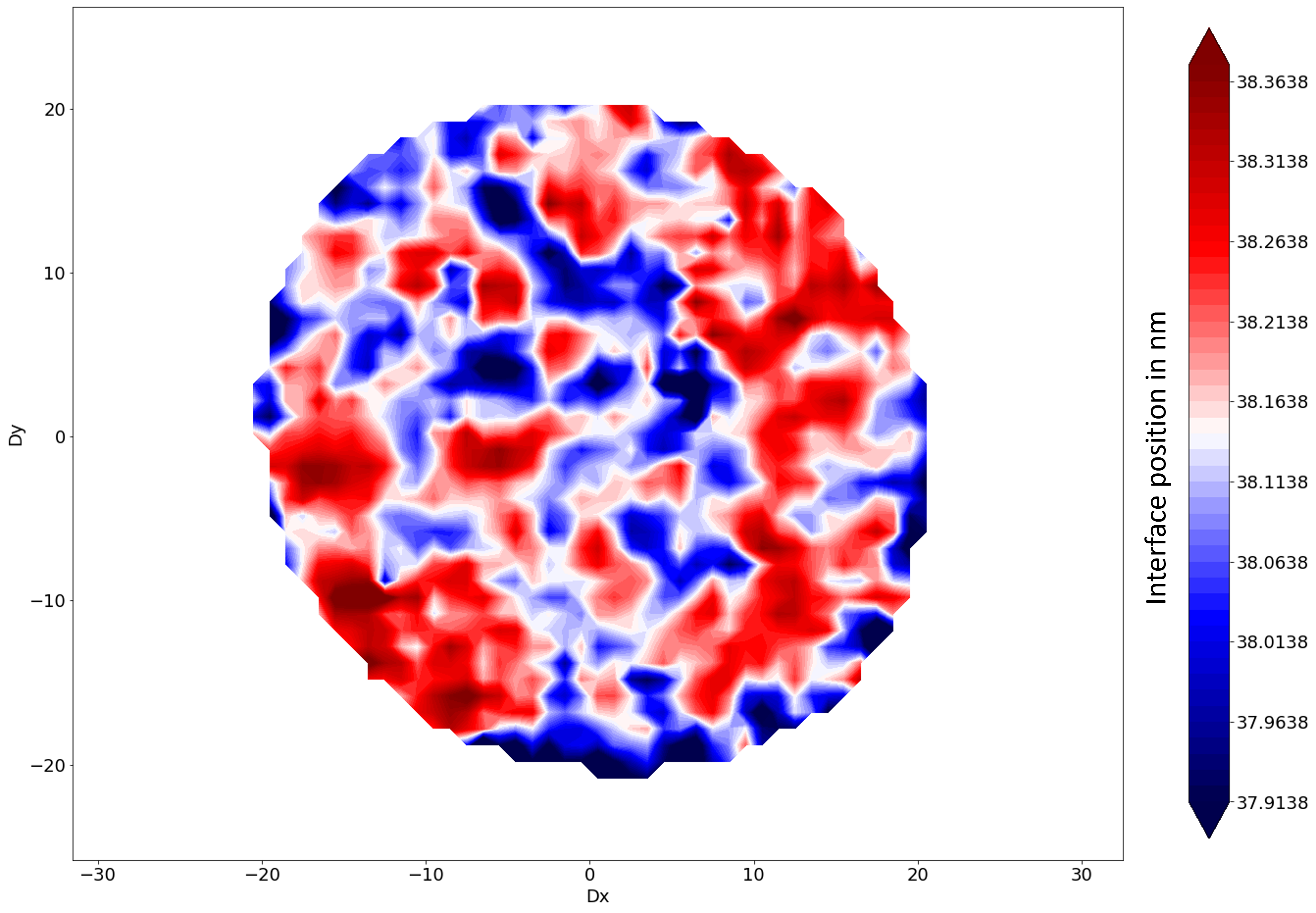
Abstract: Atom probes generate three-dimensional atomic-scale tomographies of material volumes corresponding to the size of modern-day solid-state devices. Here, the capabilities of atom probe tomography are evaluated to analyze buried interfaces in semiconductor heterostructures relevant for electronic and quantum devices. Employing brute-force search, the current dominant reconstruction protocol to generate tomographic three-dimensional images from Atom Probe data is advanced to its limits. Using Si/SiGe heterostructure for qubits as a model system, the authors show that it is possible to extract interface properties like roughness and width that agree with transmission electron microscopy observations on the sub-nanometer scale in an automated and highly reproducible manner. The demonstrated approach is a versatile method for atomic-scale characterization of buried interfaces in semiconductor heterostructures.
A method to find the best reconstruction for an interface imaged in APT and a method to map such interfaces are introduced.
Publisher Website
arXiv preprint
S. Assali, S. Koelling, Z. Abboud, J. Nicolas, A. Attiaoui, and O. Moutanabbir
Department of Engineering Physics, École Polytechnique de Montréal, C. P. 6079, Succ. Centre-Ville, Montréal, Québec H3C 3A7, Canada
Abstract: Ge/SiGe multi-quantum well heterostructures are highly sought-after for silicon-integrated optoelectronic devices operating in the broad range of the electromagnetic spectrum covering infrared to terahertz wavelengths. However, the epitaxial growth of these heterostructures at a thickness of a few micrometers has been a challenging task due to the lattice mismatch and its associated instabilities resulting from the formation of growth defects. To elucidate these limits, we outline herein a process for the strain-balanced growth on silicon of 11.1/21.5 nm Ge/Si0.18Ge0.82 superlattices (SLs) with a total thickness of 16 μm corresponding to 500 periods. Composition, thickness, and interface width are preserved across the entire SL heterostructure, which is an indication of limited Si–Ge intermixing. High crystallinity and low defect density are obtained in the Ge/Si0.18Ge0.82 layers; however, the dislocation pileup at the interface with the growth substrate induces micrometer-long cracks on the surface. This eventually leads to significant layer tilt in the strain-balanced SL and in the formation of millimeter-long, free-standing flakes. These results confirm the local uniformity of structural properties and highlight the critical importance of threading dislocations in shaping the wafer-level stability of thick multi-quantum well heterostructures required to implement effective silicon-compatible Ge/SiGe photonic devices.
Atom Probe Tomography was used to map the elemental concentrations and determine the interface steepness in a GeSi/Ge superlattice
Publisher website
arXiv preprint
Simone Assali, Anis Attiaoui, Patrick Del Vecchio, Samik Mukherjee, Jérôme Nicolas, and Oussama Moutanabbir
Department of Engineering Physics, École Polytechnique de Montréal, Montréal, Montréal, Québec, Canada H3C 3A7
Abstract: The quiet quantum environment of holes in solid-state devices is at the core of increasingly reliable architectures for quantum processors and memories. However, due to the lack of scalable materials to properly tailor the valence band character and its energy offsets, the precise engineering of light-hole (LH) states remains a serious obstacle toward coherent optical photon–spin interfaces needed for a direct mapping of the quantum information encoded in photon flying qubits to stationary spin processors. Herein, to alleviate this long-standing limitation, an all-group-IV low-dimensional system is demonstrated, consisting of a highly tensile strained germanium quantum well grown on silicon allowing new degrees of freedom to control and manipulate the hole states. Wafer-level, high bi-isotropic in-plane tensile strain (<1%) is achieved using strain-engineered, metastable germanium–tin alloyed buffer layers yielding quantum wells with LH ground state, high g-factor anisotropy, and a tunable splitting of the hole sub-bands. The epitaxial heterostructures display sharp interfaces with sub-nanometer broadening and show room-temperature excitonic transitions that are modulated and extended to the mid-wave infrared by controlling strain and thickness. This ability to engineer quantum structures with LH selective confinement and controllable optical response enables manufacturable silicon-compatible platforms relevant to integrated quantum communication and sensing technologies.
Atom Probe Tomography was used to map the Sn contamination and interface sharpness of a tensile strained Ge/GeSn quantum well.
Publisher Website
arXiv preprint
S. Assali, A. Attiaoui, S. Koelling, M. R. M. Atalla, A. Kumar, J. Nicolas, F. A. Chowdhury, C. Lemieux-Leduc, and O. Moutanabbir
Department of Engineering Physics, École Polytechnique de Montréal, C. P. 6079, Succ. Centre-Ville, Montréal, Québec H3C 3A7, Canada
Abstract: A true monolithic infrared photonics platform is within reach if strain and bandgap energy can be independently engineered in SiGeSn semiconductors. Herein, we investigate the structural and optoelectronic properties of a 1.5 μm-thick Si0.06Ge0.90Sn0.04 layer that is nearly lattice-matched to a Ge on Si substrate. Atomic-level studies demonstrate high crystalline quality and uniform composition and show no sign of short-range ordering and clusters. Room-temperature spectroscopic ellipsometry and transmission measurements show direct bandgap absorption at 0.83 eV and a reduced indirect bandgap absorption at lower energies. Si0.06Ge0.90Sn0.04 photoconductive devices operating at room temperature exhibit dark current and spectral responsivity (1 A/W below 1.5 μm wavelengths) similar to Ge on Si devices, with the advantage of a near-infrared bandgap tunable by alloy composition. These results underline the relevance of SiGeSn semiconductors in implementing a group IV material platform for silicon-integrated infrared optoelectronics.
Atom Probe Tomography was used to map the concentrations and three-dimensional distribution of elements in a Silicon-Germanium-Tin layer
Anis Attiaoui(1), Gabriel Fettu(1), Samik Mukherjee(1), Matthias Bauer(2), and Oussama Moutanabbir(1)
1 Department of Engineering Physics, École Polytechnique de Montréal, Montréal, Montréal, Québec, Canada H3C 3A7
2 Applied Materials Inc., 974 E. Arques Avenue, Sunnyvale, California 94085, United States
Abstract: Interfaces are ubiquitous in semiconductor low-dimensional systems used in electronics, photonics, and quantum computing. Understanding their atomic-level properties has thus been crucial to controlling the basic behavior of heterostructures and optimizing the device performance. Herein, we demonstrate that subnanometer interfacial broadening in heterostructures induces localized energy states. This phenomenon is predicted within a theory incorporating atomic-level interfacial details obtained by atom probe tomography. The experimental validation is achieved using heteroepitaxial (Si1–xGe,sub>x)m/(Si)m superlattices as a model system demonstrating the existence of additional paths for hole–electron recombination. These predicted interfacial electronic transitions and the associated absorptive effects are evaluated at variable superlattice thickness and periodicity. By mapping the energy of the critical points, the optical transitions are identified between 2 and 2.5 eV, thus extending the optical absorption to lower energies. This phenomenon is shown to provide an optical fingerprint for a straightforward and nondestructive probe of the subnanometer broadening in heterostructures.
Atom Probe Tomography was used to determine the interface sharpness in Si/SiGe multilayers.
Publisher Website
arXiv preprint
Lu Luo(1), Simone Assali(1), Mahmoud R. M. Atalla(1), Sebastian Koelling(1), Anis Attiaoui(1), Gérard Daligou(1), Sara Martí(2), Jordi Arbiol (2,3), and Oussama Moutanabbir(1)
1 Department of Engineering Physics, École Polytechnique de Montréal, Montréal, Montréal, Québec, Canada H3C 3A7
2 Catalan Institute of Nanoscience and Nanotechnology (ICN2), CSIC and BIST, Campus UAB, Bellaterra, 08193 Barcelona, Catalonia, Spain
3 ICREA, Pg. Lluís Companys 23, 08010 Barcelona, Catalonia, Spain
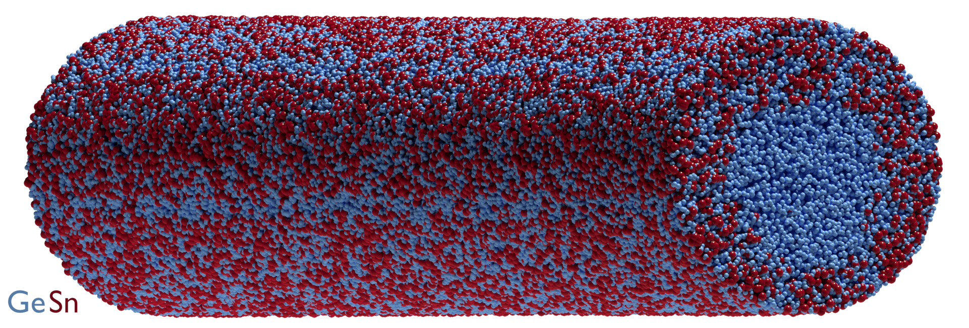
Abstract: Group IV Ge1–xSnx semiconductors hold the premise of enabling broadband silicon-integrated infrared optoelectronics due to their tunable band gap energy and directness. Herein, we exploit these attributes along with the enhanced lattice strain relaxation in Ge/Ge0.92Sn0.08 core/shell nanowire heterostructures to implement highly responsive room-temperature short-wave infrared nanoscale photodetectors. Atomic-level studies confirm the uniform shell composition and its higher crystallinity with respect to thin films counterparts. The demonstrated Ge/Ge0.92Sn0.08 p-type field-effect nanowire transistors exhibit superior optoelectronic properties achieving simultaneously relatively high mobility, high ON/OFF ratio, and high responsivity, in addition to a broadband absorption in the short-wave infrared range. Indeed, the reduced band gap of the Ge0.92Sn0.08 shell yields an extended cutoff wavelength of 2.1 μm, with a room-temperature responsivity reaching 2.7 A/W at 1550 nm. These results highlight the potential of Ge/Ge1–xSnx core/shell nanowires as silicon-compatible building blocks for nanoscale-integrated infrared photonics.
Atom Probe Tomography was used to map the Sn distribution in Ge/Ge1–xSnx core/shell nanowires.
Publisher website
arXiv preprint
Mahmoud R. M. Atalla, Simone Assali, Sebastian Koelling, Anis Attiaoui, and Oussama Moutanabbir
Department of Engineering Physics, École Polytechnique de Montréal, Montréal, Montréal, Québec, Canada H3C 3A7
Abstract: The availability of high-frequency pulsed emitters in the 2–2.5 μm wavelength range paved the way for a wealth of new applications in ultrafast spectroscopy, free-space and fiber-optical communications, surveillance and recognition, artificial intelligence, and medical imaging. However, developing these emerging technologies and their large-scale use depend on the availability of high-speed, low-noise, and cost-effective photodetectors. With this perspective, here we demonstrate GeSn photodiodes grown on silicon wafers featuring a high broadband operation covering the extended-SWIR range with a peak responsivity of 0.3 A/W at room temperature. These GeSn devices exhibit a high bandwidth reaching 7.5 GHz at 5 V bias with a 2.6 μm cutoff wavelength, and their integration in ultrafast time-resolved spectroscopy applications is demonstrated. In addition to enabling time-resolved electroluminescence at 2.3 μm, the high-speed operation of GeSn detectors was also exploited in the diagnostics of ultrashort pulses of a supercontinuum laser with a temporal resolution in the picosecond range at 2.5 μm. Establishing these capabilities highlights the potential of manufacturable GeSn photodiodes for silicon-integrated high-speed extended-SWIR applications.
Atom Probe Tomography was used to map the Sn and doping distribution in an all-GeSn PIN heterostructure.
Publisher Website
arXiv preprint
Pujitha Perla(1,2), Anton Faustmann(1,2), Sebastian Kölling(3), Patrick Zellekens(1,2), Russell Deacon(4), H. Aruni Fonseka (5), Jonas Kölzer(1,2), Yuki Sato(1,2,6), Ana M. Sanchez(5), Oussama Moutanabbir(3), Koji Ishibashi (4), Detlev Grützmacher(1,7,2), Mihail Ion Lepsa(7,2), and Thomas Schäpers(1,2)
1 Peter Grünberg Institut (PGI-9), Forschungszentrum Jülich, 52425 Jülich, Germany
2 JARA-Fundamentals of Future Information Technology, Forschungszentrum Jülich and RWTH Aachen University, 52425 Jülich, Germany
3 Department of Engineering Physics, École Polytechnique de Montréal, C.P. 6079, Succ. Centre-Ville, Montréal, Québec, Canada H3C 3A7
4 RIKEN Center for Emergent Matter Science and Advanced Device Laboratory, 351-0198 Saitama, Japan
5 Department of Physics, University of Warwick, Coventry CV4 7AL, United Kingdom
6 Faculty of Science and Engineering Department of Electronics, Doshisha University, Doshisha University, Kyotanabe, Kyoto 610-0321, Japan
7 Peter Grünberg Institut (PGI-10), Forschungszentrum Jülich, 52425 Jülich, Germany

Abstract: Semiconductor nanowires have emerged as versatile components in superconducting hybrid devices for Majorana physics and quantum computing. Th e transport properties of nanowires can be tuned either by field effect or doping. We investigated a series of InAs nanowires the conductivity of which has been modified by n-type doping using tellurium. In addition to electron microscopy studies, the wires were also examined with atomic probe tomography to obtain information about the local incorporation of Te atoms. It was found that the Te atoms mainly accumulate in the core of the nanowire and at the corners of the {110} side facets. The efficiency of n-type doping was also confirmed by transport measurements. As a demonstrator hybrid device, a Josephson junction was fabricated using a nanowire as a weak link. The corresponding measurements showed a clear increase of the critical current with increase of the dopant concentration.
Atom Probe Tomography was used to image the distribution of Tellurium dopants in InAs Nanowires grown by Molecular Beam Epitaxy
Sander G. Schellingerhout(1), Eline J. de Jong(1), Maksim Gomanko(2), Xin Guan(1), Yifan Jiang(2), Max S. M. Hoskam(1), Jason Jung(1), Sebastian Koelling(3), Oussama Moutanabbir(3), Marcel A. Verheijen(1), Sergey M Frolov(2) and Erik P. A. M. Bakkers(1)
1 Applied Physics Department, Eindhoven University of Technology
2 Department of Physics and Astronomy, University of Pittsburgh
3 Department of Engineering Physics, Ecole Polytechnique de Montréal

Abstract: Advances in quantum technology may come from the discovery of new materials systems that improve the performance or allow for new functionality in electronic devices. Lead telluride (PbTe) is a member of the group IV–VI materials family that has significant untapped potential for exploration. Due to its high electron mobility, strong spin–orbit coupling and ultrahigh dielectric constant it can host few-electron quantum dots and ballistic quantum wires with opportunities for control of electron spins and other quantum degrees of freedom. Here, we report the fabrication of PbTe nanowires by molecular beam epitaxy. We achieve defect-free single crystalline PbTe with large aspect ratios up to 50 suitable for quantum devices. Furthermore, by fabricating a single nanowire field effect transistor, we attain bipolar transport, extract the bandgap and observe Fabry–Pérot oscillations of conductance, a signature of quasiballistic transmission.
Atom Probe Tomography was used to detect and quantify Selenium contaminations in PbTe Nanowires grown by Molecular Beam Epitaxy
Ghada Badawy(1), Bomin Zhang(2), Tomáš Rauch(3), Jamo Momand(4), Sebastian Koelling(5), Jason Jung(1), Sasa Gazibegovic(1), Oussama Moutanabbir(5), Bart J. Kooi(4), Silvana Botti(3), Marcel A. Verheijen(6), Sergey M. Frolov(2), Erik P. A. M. Bakkers(1)
1 Applied Physics Department, Eindhoven University of Technology
2 Department of Physics and Astronomy, University of Pittsburgh
3 Institut für Festkörpertheorie und –optik, Friedrich-Schiller-Universität Jena
4 Zernike Institute for Advanced Materials, University of Groningen
5 Department of Engineering Physics, Ecole Polytechnique de Montréal
6 Eurofins Material Science Netherlands

Abstract: Indium antimonide (InSb) nanowires are used as building blocks for quantum devices because of their unique properties, that is, strong spin-orbit interaction and large Landé g-factor. Integrating InSb nanowires with other materials could potentially unfold novel devices with distinctive functionality. A prominent example is the combination of InSb nanowires with superconductors for the emerging topological particles research. Here, the combination of the II–VI cadmium telluride (CdTe) with the III–V InSb in the form of core–shell (InSb–CdTe) nanowires is investigated and potential applications based on the electronic structure of the InSb–CdTe interface andthe epitaxy of CdTe on the InSb nanowires are explored. The electronic structure of the InSb–CdTe interface using density functional theory is determined and a type-I band alignment is extracted with a small conduction band offset (⩽0.3 eV). These results indicate the potential application of these shells for surface passivation or as tunnel barriers in combination with superconductors. In terms of structural quality, it is demonstrated that the lattice-matched CdTe can be grown epitaxially on the InSb nanowires without interfacial strain or defects. These shells do not introduce disorder to the InSb nanowires as indicated by the comparable field-effect mobility measured for both uncapped and CdTe-capped nanowires.
Atom Probe Tomography was used to investigate the epitaxial interface between CdTe and InSb in core-shell nanowires and inform their growth
Publisher website
arXiv preprint
Samik Mukherjee, Simone Assali, and Oussama Moutanabbir
Department of Engineering Physics, École Polytechnique de Montréal, Montréal, Montréal, Québec, Canada H3C 3A7
Abstract: Using GeSn semiconductor as a model system, this work unravels the atomic-level details of the behavior of solutes in the vicinity of a dislocation prior to surface segregation in strained, metastable thin layers. The dislocations appear in the 3D atom probe tomography maps as columnar regions, 3.5–4.0 nm wide, with solute concentrations 3–4 times higher than the sounding matrix. During the initial stage of phase separation, the migration of solute atoms toward the dislocation is associated with a gradual increase in Sn concentration and in density of atomic clusters, which reach 175–190 per 103 nm3 with 12–15 atoms/cluster close to dislocations. The latter provide, at advanced stages, fast diffusive channels for Sn mass-transport to the surface, thus bringing the matrix around the dislocation to the equilibrium concentration. In parallel, an increase in solute concentration (∼0.05 at. %/nm) and in the number of atomic clusters (12–16 clusters/33 nm) is observed along the dislocation core.
Atom Probe Tomography was used to map the Sn enrichment in dislocations of GeSn crystals.
Jaswant Rathore(1), Alisha Nanwani(1), Samik Mukherjee(2), Sudipta Das(1), Oussama Moutanabbir(2), and Suddhasatta Mahapatra(1)
1 Department of Physics, Indian Institute of Technology Bombay, Mumbai 400076, India
2 Department of Engineering Physics, École Polytechnique de Montréal, Montréal, Montréal, Québec, Canada H3C 3A7
Abstract: We systematically investigate the compositional uniformity, degree of strain relaxation (DSR), defect structure and surface morphology of GeSn epitaxial layers with 16% Sn, grown by low temperature molecular beam epitaxy (MBE) on Ge-buffered Si(001) substrates. Combining atom probe tomography, reciprocal space mapping, cross-sectional transmission electron microscopy, and atomic force microscopy analyses, we demonstrate that for a layer thickness of tGeSn=250 nm, a high DSR (70%) can be achieved, while maintaining compositional uniformity at the atomic scale. We find no evidence of Sn clustering in the bulk, or Sn segregation to the surface, for at least this value of tGeSn. The observed compositional uniformity contrasts the well-established phenomenon of strain-relaxation enhancement of Sn content in chemical vapour deposition (CVD) growth of GeSn. The defect structure leading to strain relaxation in these MBE-grown GeSn epitaxial layers is also distinctly different from that observed in CVD growth of the alloy. We observe the co-existence of highly strain-relaxed and pseudomorphically strained regions in the grown epilayers, tentatively explained by bunching of threading dislocations. Considering that MBE growth of GeSn epitaxial layers, with such high-Sn content and layer thickness, has not been reported before, our results are encouraging for future improvements in design and fabrication of group-IV-based mid-infrared photonic devices.
Atom Probe Tomography was used to map the Sn distribution in GeSn layers.
Sebastian Koelling(1), Simone Assali(1), and Oussama Moutanabbir(1)
1 Department of Engineering Physics, Polytechnique Montréal, C. P. 6079, Montréal, Québec H3C 3A7, Canada

Abstract: Atom Probe Tomography (APT) has significantly advanced our ability to characterize buried interfaces and to map the three-dimensional distribution of atomic constituents like dopants in modern day electronic nano-devices. This precise mapping of the chemical composition and buried interfaces is also highly sought-after in the implementation and optimization of a variety of emerging photonic devices with dimensions of up to several micrometers as opposed to the few ten nanometers of modern day transistors. Herein, we show that APT is poised to contribute to the development of these devices by adapting the Focused Ion beam based preparation of APT specimen, typically used for preparing semiconductor samples. Using in-situ grown nanowires as sacrificial masks during specimen preparation, we demonstrate APT analyses of micrometer-sized volumes of semiconductor heterostructures.
A method to prepare samples for Atom Probe Tomography using an electron beam deposited hard-mask in a Focused Ion-/Electron Dual Beam tool is introduced
Publisher website
arXiv preprint
T. Grange(1), S. Mukherjee(2), G. Capellini(3,4), M. Montanari(4), L. Persichetti(4), L. Di Gaspare(4), S. Birner(1), A. Attiaoui(2), O. Moutanabbir(2), M. Virgilio(5), and M. De Seta(4)
1 Nextnano GmbH, Garching b., München 85748, Germany
2 Department of Engineering Physics, École Polytechnique de Montréal, Montreal, Quebec, Canada
3 IHP – Leibniz-Institut für innovative Mikroelectronik, Im Technologiepark 25, 15236 Frankfurt (Oder), Germany
4 Dipartimento di Scienze, Università degli Studi Roma Tre, 00146, Roma, Italy
5 Dipartimento di Fisica “E. Fermi”, Università di Pisa, Largo Pontecorvo 3, 56127 Pisa, Italy
Abstract: In this manuscript, we develop a generalized theory for the scattering process produced by interface roughness on charge carriers that is suitable for any semiconductor heterostructure. By exploiting our experimental insights into the three-dimensional atomic landscape of Ge/Ge-Si heterointerfaces obtained by atom probe tomography, we are able to define the full set of interface parameters relevant to the scattering potential, including both the in-plane and axial correlation inside real diffuse interfaces. Our experimental findings indicate a partial coherence of the interface roughness along the growth direction within the interfaces. We show that it is necessary to include this feature, previously neglected by theoretical models, when heterointerfaces characterized by finite interface widths are taken into consideration. To show the relevance of our generalized scattering model in the physics of semiconductor devices, we implement it in a nonequilibrium Green’s function simulation platform to assess the performance of a Ge/Si-Ge-based terahertz quantum cascade laser.
Atom Probe Tomography was investigate the interface sharpness in SiGe superlattices.
Publisher website
arXiv preprint
Jérôme Nicolas(1), Simone Assali(1), Samik Mukherjee(1), Andriy Lotnyk(2), Oussama Moutanabbir(1)
1 Department of Engineering Physics, École Polytechnique de Montréal, Montréal, Montréal, Québec, Canada H3C 3A7
2 Leibniz Institute of Surface Engineering (IOM), Permoserstr. 15, 04318 Leipzig, Germany
Abstract: Epitaxial Sn-containing group-IV semiconductors (Si)GeSn relevant for optoelectronics are inherently strained and supersaturated in Sn and thus can suffer instabilities that are still to be fully elucidated. In this vein, in this work, the microstructure and atomic-scale composition of Ge0.82Sn0.18 are investigated at the onset of phase separation as the epitaxial growth aborts. In addition to the expected accumulation of Sn on the surface, leading to Sn-rich droplets and subsurface regions with the anticipated equilibrium Sn composition of 1.0 atom %, the diffusion of Sn atoms also yields conspicuous Sn-decorated filaments with nonuniform Sn content in the range of ∼1 to 11 atom %. The latter are attributed to the formation and propagation of dislocations, facilitating the Sn transport toward the surface through pipe diffusion. Furthermore, the interface between the Sn droplet and GeSn shows a distinct, defective layer with Sn content of ∼22 atom %. This layer is likely formed by the expelled excess equilibrium Ge as the Sn solidifies, and its content seems to be a consequence of strain minimization between tetragonal Sn-rich and cubic Ge-rich equilibrium phases. The elucidation of these phenomena is crucial to understand the stability of GeSn semiconductors and control their epitaxial growth at a uniform composition.
Atom Probe Tomography was used to image Sn segregation in GeSn crystals.
Publisher website
arXiv preprint
Samik Mukherjee(1), Anis Attiaoui(1), Matthias Bauer(2), and Oussama Moutanabbir(1)
1 Department of Engineering Physics, École Polytechnique de Montréal, Montréal, Montréal, Québec, Canada H3C 3A7
2 Applied Materials Inc., 974 E. Arques Avenue, Sunnyvale, California 94085, United States
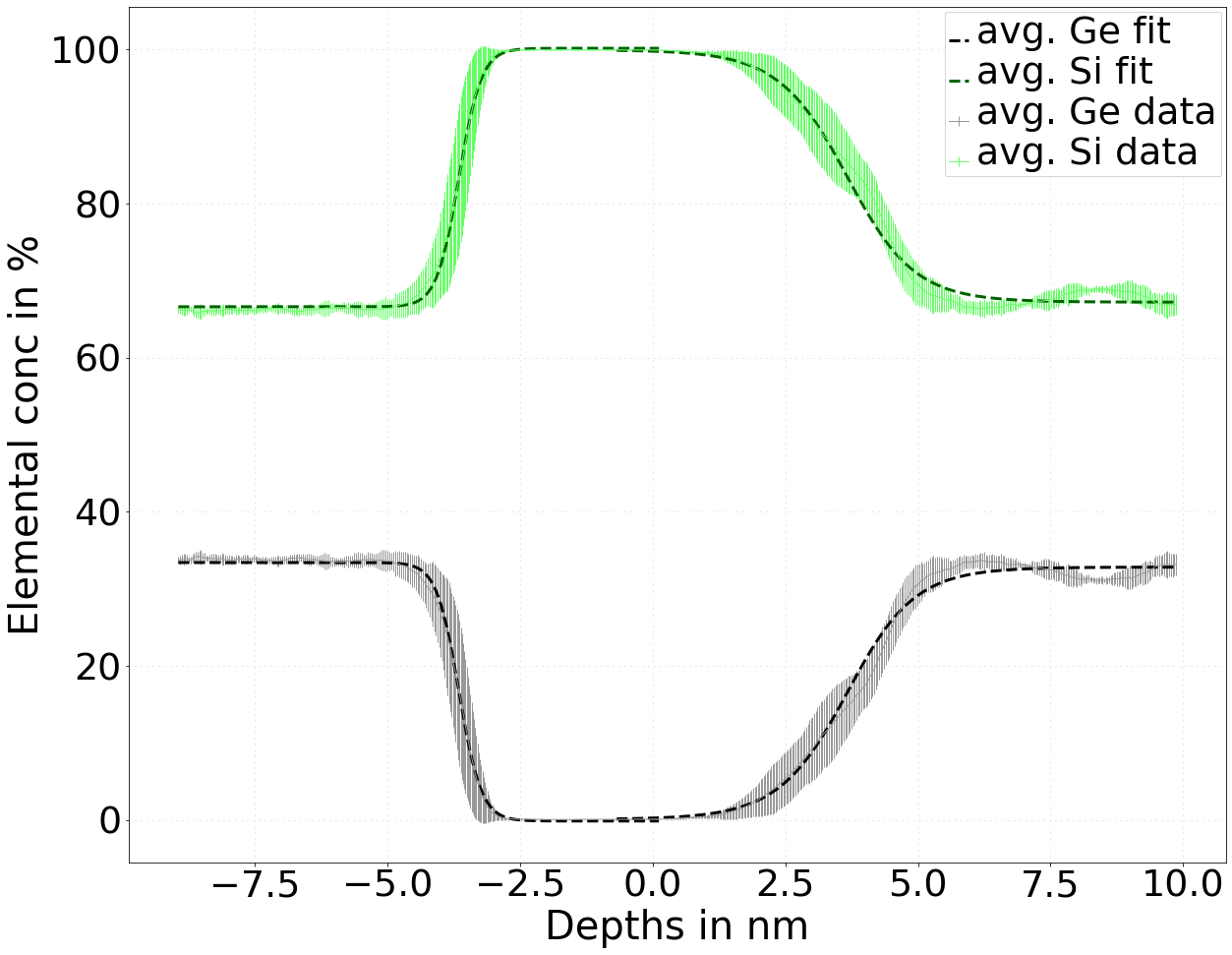
Abstract: The interfacial abruptness and uniformity in heterostructures are critical to control their electronic and optical properties. With this perspective, this work demonstrates the three-dimensional (3D) atomic-level mapping of the roughness and uniformity of buried epitaxial interfaces in Si/SiGe superlattices with a layer thickness in the 1.5–7.5 nm range. Herein, 3D atom-by-atom maps were acquired and processed to generate isoconcentration surfaces highlighting local fluctuations in content at each interface. These generated surfaces were subsequently utilized to map the interfacial roughness and its spatial correlation length. The analysis revealed that the root-mean-squared roughness of the buried interfaces in the investigated superlattices is sensitive to the growth temperature with a value varying from 0.17 ± 0.02 to 0.26 ± 0.03 nm in the temperature range of 500–650 °C. The estimated horizontal correlation lengths were found to be 8.11 ± 0.5 nm at 650 °C and 10.09 ± 0.6 nm at 500 °C. Additionally, reducing the growth temperature was found to improve the interfacial abruptness, with a 30% smaller interfacial width is obtained at 500 °C. This behavior is attributed to the thermally activated atomic exchange at the surface during the heteroepitaxy. Finally, by testing different optical models with increasing levels of interfacial complexity, it is demonstrated that the observed atomic-level roughening at the interface must be accounted for to accurately describe the optical response of Si/SiGe heterostructures.
Atom Probe Tomography was used to determine the interface sharpness in Si/SiGe multilayers.
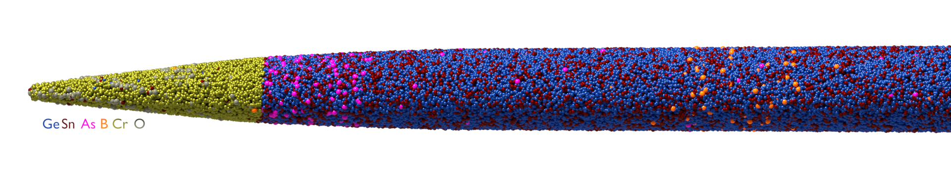
Lu Luo, Mahmoud R. M. Atalla, Simone Assali, Sebastian Koelling, Anis Attiaoui, and Oussama Moutanabbir
Department of Engineering Physics, École Polytechnique de Montréal, C P. 6079, Succ. Centre-Ville, Montréal, Québec, Canada
Abstract: Ge/GeSn core/shell nanowire (NW) photodetectors operating at room-temperature will be demonstrated with a cutoff wavelength that can be precisely tuned from ~2 μm (8 at.% Sn) to longer MIR wavelengths (~18 at.% Sn) by controlling the Sn content in the shell.
Atom Probe Tomography was used to map the elemental distribution in Ge/GeSn core-shell nanowires.
Merritt P. Losert(1), Brian Paquelet Wuetz(2), Sebastian Koelling(3), Lucas Stehouwer(2), Anne-Marije Zwerver(2), Stephan G. Philips(2), Mateusz Madzik(2), Xiao Xue(2), Guoji Zheng(2), Mario Lodari(2), Sergey V. Amitonov(2), Nodar Samkharadze(2), Amir Sammak(2), Lieven Vandersypen(2), Rajib Rahman(4), Sue N. Coppersmith(4), Oussama Moutanabbir(3), Mark G. Friesen(1), Giordano Scappucci(2)
1 University of Wisconsin-Madison
2 QuTech and Kavli Institute of Nanoscience, Delft University of Technology
3 Department of Engineering Physics, École Polytechnique de Montréal
4 University of New South Wales
Abstract: We present a theory of how alloy disorder affects the intervalley coupling and valley splitting in quantum dot qubits in Si/SiGe heterostructures. We show that this theory is in good agreement with experiments as well as the NEMO-3D 20-band strain-dependent sp3d5s* tight-binding model. We find that, for realistic devices, alloy disorder is the dominant source of variation in the valley splitting. Moreover, we show that increasing the alloy disorder increases the spread of the intervalley coupling, thereby increasing the average valley splitting. These results lead to a new and counterintuitive strategy for engineering quantum wells with large average valley splittings: increasing the alloy disorder. We find that adding just 5% Ge to the bottom of the quantum well enhances valley splittings substantially, achieving splittings larger than 100 μeV over 95% of the time. This strategy runs counter to the prevailing strategy of making devices with little disorder and very sharp interfaces
Atom Probe Tomography was used support the modeling of electrostatically defined qubits in strained 28Si quantum wells.
Badawy, Ghada; Zhang, Bomin; Rauch, Tomas; Momand, Jamo; Koelling, Sebastian; Moutanabbir, Oussama; Kooi, Bart; Botti, Silvana; Verheijen, Marcel; Frolov, Sergey; Bakkers, Erik P. A. M.
Abstract: Indium antimonide (InSb) nanowires are considered prime candidates for the emergent semiconducting-superconducting hybrids used for the topological Majorana particles research. A common concern in current nanowire devices is the overly strong superconducting-semiconducting coupling, which tends to overwhelm the intrinsic properties of the semiconducting nanowire. It has been proposed that adding a tunnel barrier at the nanowire-superconductor interface modulates this coupling. Here, we add cadmium telluride (CdTe) shells around the InSb nanowires and investigate their suitability to serve as a tunnel barrier between a superconductor and InSb nanowires based on the electronic structure of the InSb-CdTe interface, the growth, and epitaxy of the CdTe on InSb. We use density functional theory to extract the individual bandgaps of InSb and CdTe as well as the band alignment at the interface. Moreover, we demonstrate that these insulating, lattice matched CdTe shells can be grown epitaxially on the InSb nanowires without interfacial strain or defects. The obtained defect-free and epitaxial interfaces along with the control over shell thickness we achieve indicate the potential of these CdTe shells to act as a control knob that tunes the superconducting-semiconducting coupling.
Atom Probe Tomography was used to investigate the epitaxial interface between CdTe and InSb in core-shell nanowires and inform their growth.
Lu Luo, Simone Assali, Mahmoud R. M. Atalla, Sebastian Koelling, and Oussama Moutanabbir
Ecole Polytechnique de Montreal
Abstract: Germanium-Tin (GeSn) alloys have recently been the subject of extensive investigations as new material systems to engineer a direct bandgap in group IV semiconductors, which will pave the way to developing silicon-compatible photonic, electronic and optoelectronic devices. The same paradigm can be extended to grow nanowires (NWs) and NW heterostructures, thus providing additional degrees of freedom to tailor the basic properties of this emerging class of semiconductors. Careful control of the growth kinetics to incorporate Sn atoms into Ge at concentrations about one order of magnitude higher than the equilibrium solubility is at the core of this technology. In this presentation, we will discuss the structural and opto-electronic properties of Ge/GeSn core/shell nanowires (NW) that are grown with a tunable, uniform Sn content exceeding 20 at.%. Single NW photodetectors operating at short-wave infrared (SWIR) and mid-infrared (MIR) wavelengths will be shown at room temperature and their properties will be investigated at cryogenic temperatures. By simultaneously increasing Sn content and minimizing strain in the GeSn shell, the absorption edge in the photocurrent measurements can be precisely tuned from ~2 μm (8 at.%) to longer MIR wavelengths.
Atom Probe Tomography was used to map the Ge and Sn distribution in Ge/GeSn core-shell nanowires.
Conference Website
Brian Paquelet Wuetz, Merritt Losert, Sebastian Koelling, Anne-Marije Zwerver, Lucas Stehouwer, Nodar Samkharadze, Stephan Philips, Mateusz Madzik, Guoji Zheng, Xiao Xue, Sergei Amitonov, Mario Lodari, Amir Sammak, Susan Coppersmith, Lieven Vandersypen, Oussama Moutanabbir, Mark Friesen, Giordano Scappucci
 Abstract: 28Si/SiGe heterostructures provide a compelling host material for a scalable quantum computer, due to the long coherence times of spin qubits and compatibility with industry. Here we study 28Si/SiGe heterostructures with varying roughness of the critical Si/SiGe interfaces to understand the energy splitting of the lowest lying conduction valleys (valley splitting). To improve control of valley splitting in 28Si/SiGe, we implement a feedback cycle for materials stack engineering including several elements. We use atom probe tomography to provide atomic 3D reconstruction of the material stack and statistical understanding of compositional variations at the Si/SiGe interface over nanoscale dimensions relevant for spin qubits. The resulting data is fed into a tight binding model to compute the valley splitting in real quantum wells with varying thickness, Si/SiGe interface width, and interface chemical roughness. We complete the cycle by comparing the simulation results with valley splitting measured in heterostructure field effect transistors and quantum dots, making use of cryomultiplexer technology to achieve statistically significant metrics. We envision that such a feedback loop may help to engineer optimal stacks for large and controllable values of valley splitting in Si/SiGe.
Atom Probe Tomography was used to map Ge distribution and Si isotope distribution in a strained 28Si quantum well layers sandwiched between SiGe layers.
Abstract: 28Si/SiGe heterostructures provide a compelling host material for a scalable quantum computer, due to the long coherence times of spin qubits and compatibility with industry. Here we study 28Si/SiGe heterostructures with varying roughness of the critical Si/SiGe interfaces to understand the energy splitting of the lowest lying conduction valleys (valley splitting). To improve control of valley splitting in 28Si/SiGe, we implement a feedback cycle for materials stack engineering including several elements. We use atom probe tomography to provide atomic 3D reconstruction of the material stack and statistical understanding of compositional variations at the Si/SiGe interface over nanoscale dimensions relevant for spin qubits. The resulting data is fed into a tight binding model to compute the valley splitting in real quantum wells with varying thickness, Si/SiGe interface width, and interface chemical roughness. We complete the cycle by comparing the simulation results with valley splitting measured in heterostructure field effect transistors and quantum dots, making use of cryomultiplexer technology to achieve statistically significant metrics. We envision that such a feedback loop may help to engineer optimal stacks for large and controllable values of valley splitting in Si/SiGe.
Atom Probe Tomography was used to map Ge distribution and Si isotope distribution in a strained 28Si quantum well layers sandwiched between SiGe layers.Simone Assali, Mahmoud R. M. Atalla, Anis Attiaoui, Sebastian Koelling, Gérard Tanguy Eric Gnato Daligou, and Oussama Moutanabbir
Ecole Polytechnique de Montreal
Abstract: Si-compatible photonic and opto-electronic devices operating at MIR wavelengths can now be fabricated using Sn-rich group IV semiconductor SiGeSn alloys, directly grown on a Si substrate. The possibility to independently engineer strain and composition in this new class of semiconductors allows for a high degree of tunability of band structure and lattice parameter of the material, thus enabling a variety of multi-layer heterostructures and low-dimensional systems. In this presentation, the recent progress in the non-equilibrium epitaxial growth of metastable (Si)GeSn semiconductors in a CVD reactor will be discussed.[1-2] Room-temperature Ge0.83Sn0.17 membrane photodetectors operating up to a wavelength of 4.6μm will be demonstrated, which lays the groundwork to implement scalable, flexible, and low-cost sensing and imaging technologies using Sn-rich group IV semiconductors.[3-4] This technology covers the MIR (3-8μm) that is commonly only accessible using expensive InSb and MCT materials. Moreover, the effect of material properties (crystalline quality, composition, point defects, dopants) will be discussed in MIR p-i-n photodetectors and LEDs.
[1]S.Assali,Appl.Phys.Lett.251903(2018)
[2]S.Assali,J.Appl.Phys.025304(2019)
[3]M.Atalla,Adv.Func.Mat(2020)
[4]S.Assali,arXiv:2004.13858
Atom Probe Tomography was used to map the Si, Ge and Sn distribution (Si)GeSn multilayers and the characterize the interface quality between the layers.
S. Koelling (1), S. Assali (1, 2), M. Atalla (1), A. Kumar (1), A. Attiaoui (1), M. Lodari (3), A. Sammak (3), G. Scappucci (3, 4), and O. Moutanabbir (1)
1 École Polytechnique de Montréal
2 Eindhoven University of Technology
3 TU Delft
4 Kavli Institute of Nanoscience Delft
Abstract: Probing the quality of interfaces, dopant distribution, layer thicknesses, and crystalline quality in buried layers and volumes has been critical for developing new semiconductor materials and devices. These challenges have been addressed by a combination of techniques based on Electron Microscopy (EM) and Atom Probe Tomography (APT) for new transistor architecture[1]. We have extended their applicability to materials and devices developed for quantum information processing[2] and photonic applications[3-5] with significantly larger dimensions addressing the need for atomic scale metrology of heterostructures with thicknesses of up to several micrometers.
For example, CMOS compatible Quantum cascade lasers based on superlattices of n-type Ge/Si1-xGex QWs are predicted to be operable at room temperature and to emit throughout the entire THz spectral region (300GHz-1THz, 1mm-30µm) solving a key challenge in solid-state optoelectronics5. In a QCLs charged carriers travel through the superlattice alternating between emitting radiation when traversing between the subbands of the superlattice and tunneling from one period of the cascade to the next[3,5]. In order to act as a laser, the underlying material structure has to allow for coherent radiation, population inversion, efficient tunneling and propagation of the emitted radiation. This implies the need to develop the growth of superlattices up to 1000s of periods that are highly uniform in thickness, strain compensated, of high crystalline quality, and have well controlled doping levels and steep interfaces reaching a thickness of several micrometers[3,5].
Here we will show how we combine X-Ray Diffraction, EM and APT to characterize Ge/Si1-xGex superlattices and SiGe-, GeSn- and SiGeSn heterostructures to investigate interface properties, determine layer thicknesses, and map the distribution of dopants and isotopes[6] in structures with micrometer dimensions. These studies are of compelling importance to enable a progressive improvement of these material systems towards their respective applications.
References:
1 W. Vandervorst et al., Phys. Status Solidi C 11, 121 (2014)
2 N.W. Hendrickx et al., Nature 577, 487 (2020)
3 D.J. Paul, Laser Photonics Rev. 4, 610-632 (2010)
4 S. Assali et al. Appl. Phys. Lett. 112, 251903 (2018)
5 T. Grange et al., Appl. Phys. Lett. 114, 111102 (2019)
6 D. Sabbagh et al., Phys. Rev. Appl. 12, 014013 (2019)
A method to prepare samples for Atom Probe Tomography using an electron beam deposited hard-mask in a Focused Ion-/Electron Dual Beam tool is introduced and analyses on micrometer thick structures for photonic applications are shown.